ELSA is a unique quasi in situ facility, developed at TU Wien by CEST to cover the multiple research areas associated with the electrochemical technologies. This facility is dedicated to unravelling the surface and interface processes of thin films. This is a one-of-its kind facility, designed to understand the electrochemical surface/interface phenomena at real operating conditions and therefore, fully equipped to characterize the sample without exposing to air (as air exposure can alter the surface properties).
Access to the Facility:
The facility is open to industrial and academic researchers, as well as business-to-business engagements. It is available for booking both short-term project measurements and long-term measurements. Furthermore, confirmation of measurement slots for project applications is available upon request.
We are also open to collaborate on proposal writing within the facility’s scope, offering our expertise in surface analysis to support the application process.
For slot bookings and inquiries regarding the instrument scope, please contact us at [office@cest.at].
Below is a detailed overview of the cluster to provide an understanding of the facility.
The unique features of ELSA include:
- Central distribution chamber
- Ultra-High Vacuum (UHV) Kelvin Probe
- Electrochemical Stations
- Scanning X-ray Photoelectron Spectroscopy (SXPS)
- Auger Electron Spectroscopy (AES)
- Vacuum suitcase for sample transfer
Research areas covered:
- Hydrogen production
- Fuel cells
- Batteries
- Recycling
- Corrosion study
Central distribution chamber
A distribution chamber featuring six ports has been employed to interconnect various UHV systems and facilitate sample transfer between them. Currently, SXPS, load lock, storage chamber, solid-liquid EC station, and a vacuum suitcase are connected to five of the ports. The sixth port will soon be connected to a PVD chamber.
Ultra-High Vacuum (UHV) Kelvin Probe
Kelvin probe is a highly surface sensitive technique used to measure the work function of a material, defined by the maximum top three atomic layers. This technique is similar to atomic force microscopy (AFM) except being a non-contact technique. ELSA is equipped with a UHV kelvin probe (Model- UHV KP020, KP Technology) to measure the work function of thin films before and after electrochemical measurements. As this technique is highly surface sensitive, we can determine surface changes (adsorption, surface reconstruction, defects, charge carrier trapping, corrosion etc.) occurring after exposure to electrolyte. One of the ports of distribution chamber is used to connect Kelvin probe which is further connected to the electrochemical (EC) station.
Electrochemical Stations
Solid/liquid interface study: An electrochemical (EC) station has been connected to the distribution chamber via Kelvin probe to carry out the quasi in-situ measurements on Solid/liquid interfaces. This chamber is dedicated to electrolysis, CO2 reduction, corrosion, and recycling applications.
Solid-electrolyte-interface (SEI) study: Second EC station is devoted for the cutting-edge research in the field of batteries and directly connected to the SXPS.
High-temperature Study: In-situ measurement up to 600 degrees Celsius is also feasible using the hot-cold sample holder at SXPS.
Scanning X-ray Photoelectron Spectroscopy (SXPS)
XPS technique is surface sensitive and used to determine the surface composition limited to the top few nm layer. It is based on the external photoelectric effect; the sample is irradiated with X-rays, which results in the emission of photoelectrons. The kinetic energy of the ejected photoelectrons reveals the elemental composition and electronic state of surface elements. That’s why this technique is also known as electron spectroscopy for chemical analysis (ESCA).
Model: PHI 5000 Versa Probe III SXPS
Specifications:
-
-
- Unique high flux X-ray source providing focused monochromatic X-ray (Al anode) beam and micro-area spectroscopy capability
- High resolution 180° spherical capacitor energy analyzer
- Scanning X-ray imaging within 1-5 seconds with fine focusing to 10 µm diameter
- Floating column monatomic argon ion gun
- Dual beam charge neutralization
- Dual Zr/Mg anode
- mu-metal test chamber for magnetic field shielding enhancement
- 20 kV Argon gas cluster ion gun beam (GCIB) with Zalar rotations minimizing the potential for chemical damage
- Reflection Electron Energy Loss Spectroscopy (REELS) allowing spectra acquisition up to 2000 eV in loss energy
- Five axis sample stage with x and y translation of ± 25 mm, z axis translation of ± 20 mm and tilt axis range of 0° to 90°
- 4 electrical contact hot/cold stage
- Camera with zoom lens to capture image in introduction chamber
- Intro ion gauge option allows vacuum level measurement up to 10-8 Pa
SXPS with above-mentioned specifications provides following information:
- Quantitative surface analysis: elemental composition, chemical formula, and electronic state of elements
- Secondary electron image allows to distinguish heterogenous surface
- Angle-dependent XPS measurement and compositional depth profiling possible
Applications:
- Thin films and coatings analysis
- Nature of interfacial layers
- Detection of dopants and impurities
- Corrosion study
Sample Requirements:
- Powder/thin film (Organic/inorganic/ Polymer)
- Nature: conducting, semi-conducting, insulating
-
Auger Spectroscopy (AES)
ELSA is equipped with AES, which is a complementary surface analysis technique. In AES technique, the sample is irradiated with a focused electron beam leads to the ejection of an inner shell electron. The vacancy of ejected electron is filled by an outer shell electron with emission of secondary X-ray. This secondary X-ray of energy equal to the energy difference between two orbitals leads to the ejection of another outer shell electron known as auger electron. The kinetic energy of auger electron is element specific and helps in evaluating the surface composition. The focused electron beam allows the analysis of ultramicroscopic area (~ 5 nm). AES provides better spatial resolution over XPS as its probe beam is relatively 100 times smaller.
Model: Scanning Auger Nanoprobe (PHI 710)
Specifications:
- Most versatile Auger analysis capability owing to the coaxial electron gun and cylindrical analyzer geometry quenching the shadowing effect
- Secondary electron imaging with 4096 by 4096 pixel resolution and fine focussing to ~3 nm.
- Floating column monatomic argon ion gun to sputter clean the sample
- Focused ion beam (FIB)
- 4 electrical contact heating stage
- Flexible five axis sample stage with x and y translation of ± 25 mm, z axis translation of ± 20 mm
- Acoustic enclosure to reduce image drift and mu-metal test chamber for magnetic field shielding enhancement
- 60 mm intro chamber
- Coupled to Oxford EDX
Applications:
- Thin films and coatings analysis
- Nature of interfacial layers (with FIB, it’s easy to investigate the surface and deeper layers at the same time)
- Detection of dopants and impurities
- Corrosion study
Sample Requirements:
- Powder/thin film (Organic/inorganic/ Polymer)
- Nature: conducting, semi-conducting, insulating
Vacuum Suitcase
ELSA is equipped with a vacuum suitcase (≤ 10-10 mbar) to integrate the system with other CEST facilities (LEIS cluster). Therefore, we can transfer the sample from ELSA lab to CEST without exposing the surface to air. Additionally, we have a small vacuum vessel from PHI electronics to transfer samples from SXPS to AES. This vessel also facilitates sample transfer from a glovebox under inert gas atmosphere.
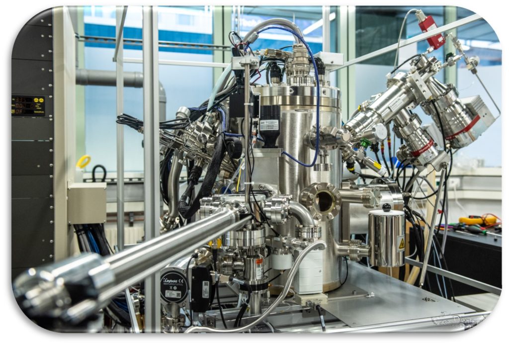
PHI 5000 Versa Probe III, ELSA Lab, TU Wien

Scanning Auger Nanoprobe (PHI 710), TU Wien