Scanning electron microscopy uses electron beams instead of light to produce the images. As a result, a significantly higher resolution is achieved. The scanning electron microscope images surfaces of samples with a three-dimensional perspective, wherein the large depth of focus is of particular importance. Electrons emitted from an electron source are condensed into a fine beam. This beam moves in a well-defined grid over the sample surface. The electrons emitted by the interaction with the primary beam from the sample surface are captured by detectors and converted into an image: the secondary electron (SE) imaging enables the representation of the topography of the sample surface; the backscattered electron (BSE) image also provides information about the different composition of the sample surface (in BSE mode: bright spots – heavier elements, dark spots – lighter elements).
Application:
- Surface topography and surface texture:
- surface roughness
- different element composition
- fracture surface characterization
- particle size determination of powders
- Structural examinations:
- particle size distribution
- phase analysis
- identification of precipitated phases
- Layer thickness determination, layer structure analysis:
- element analysis (EDX)
- crystallography, orientation, texture (EBSD)
Specifications:
- Acceleration voltage: 0.1 – 30 kV
- Resolution: point to point resolution approx. 1 nm; due to FEG also excellent resolution at low acceleration voltages
- Maximum gas pressure in sample chamber: 1.3 mbar
- (Semi) -quantitative element analysis (EDX) for elements with atomic numbers ≥ boron (EDAX-TEAM OCTANE PLUS version 4.3 system)
- Analysis of the orientation using EBSD (resolution 100 nm)
Sample requirements:
- Sample size: max. 10 x 10 cm
- Maximum sample height (for elemental analysis): 2 cm
- Sample condition: solid, powdery
Possible samples:
- Conductive surfaces: e.g. metals
- Non-conductive surfaces: plastics, ceramics, paper, etc., …
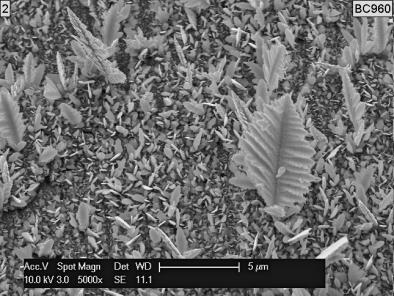
Topography and structure
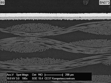
Cross-section analysis and microstructure

EBSD analysis